Target Market Segments
for 3D Circuit Printing
We want to give you the freedom
to 3D print high-resolution
or very thick electronic
circuits, bumps and bonding
layers through the AMEBA 3D
(S-ECAM for 3D Circuit) series
of machines.
01
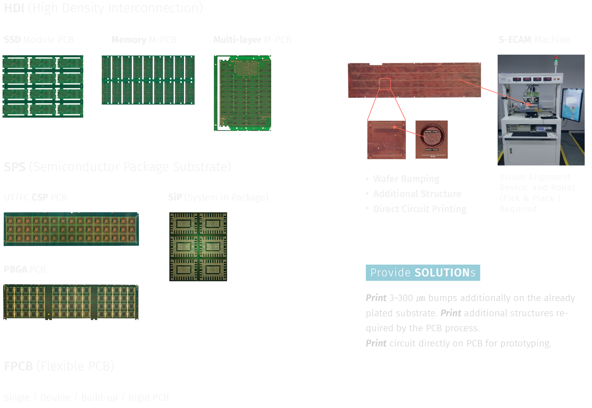
S-ECAM can print 3 ~ 300 ㎛ diameter and 10 ~ 500 ㎛ height of bumps (pillars) within the aspect ratio of 1:5 using the multi-electrode module of strip size. S-ECAM can print additional structures and spacers required by the PCB design or process demands, and it is also possible to directly print circuits on the PCB substrate for prototyping.
02
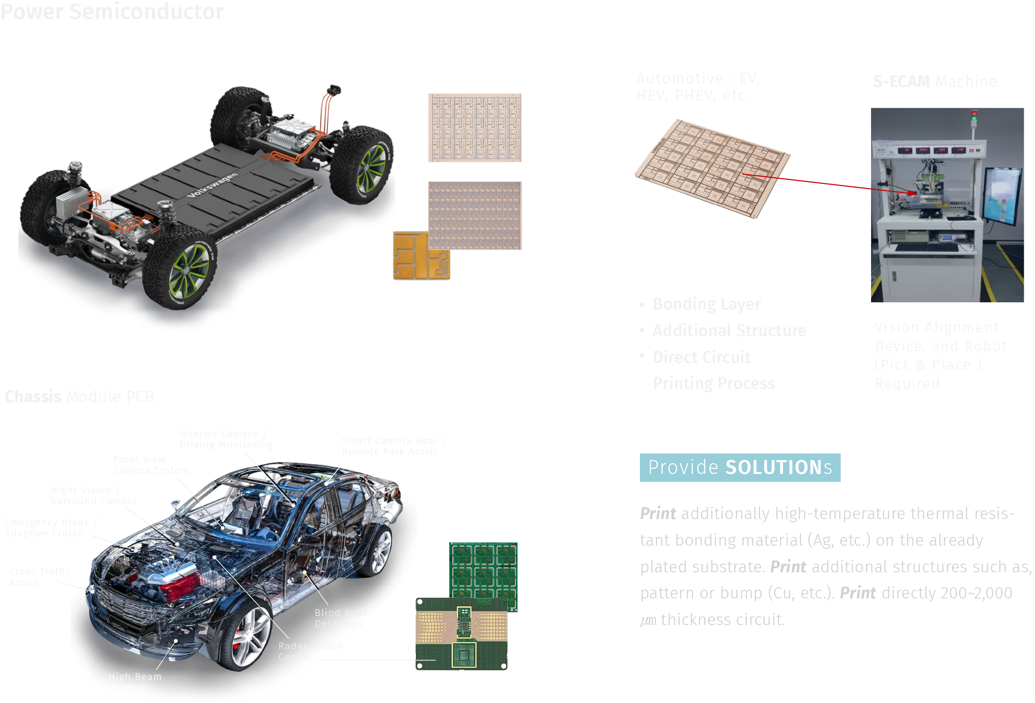
S-ECAM additionally prints a high-temperature thermal resistant bonding material such as Ag on the target area of the
substrate of ceramic PCB for high-power semiconductor in which the circuit pattern has already been manufactured.
S-ECAM can effectively print circuits with a thickness of 200 ~ 2000 ㎛ using a multi-electrode module.For this, the
DfAM (Design for Additive Manufacturing) should be performed the improvement of circuit design in advance.
Power Semiconductor
03
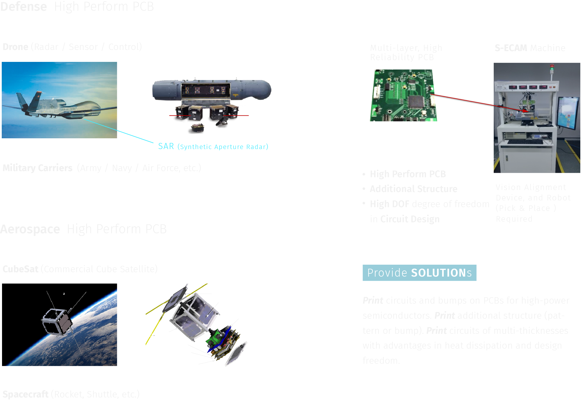
S-ECAM can print bumps or electronic circuits on high-density and high-performance PCBs required for the high-tech
electronic equipment in defense and aerospace fields. S-ECAM is capable of printing multi-thickness circuits on the
PCB substrate with advantages in terms of heat dissipation and design freedom, and it is also possible to print addi
tional 3D structures for mounting semiconductors on the PCB or the device assembly.
04
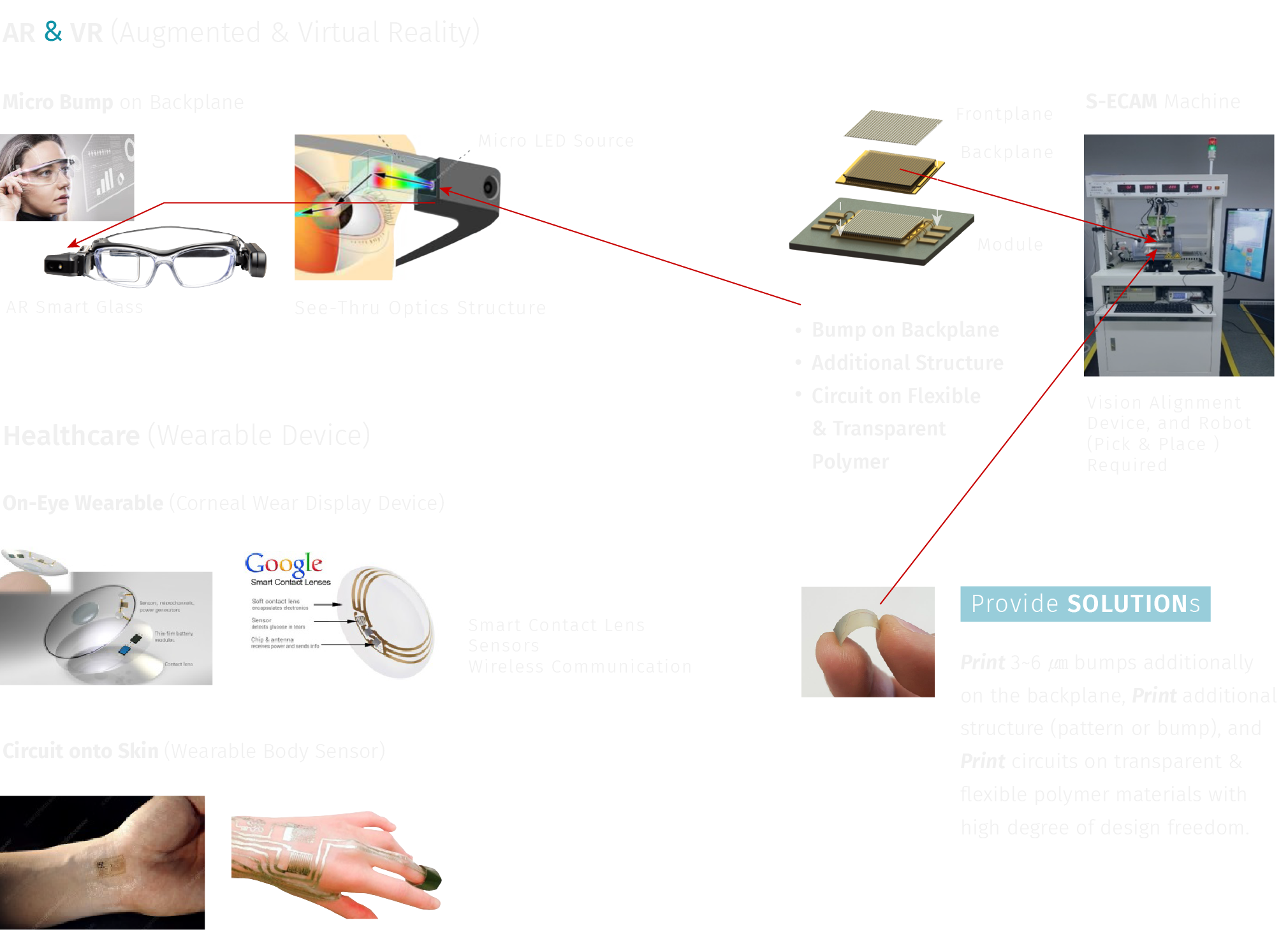
S-ECAM prints bumps with a diameter of 3 to 6 ㎛ on the backplane to enable bonding with wafers or modules that im
plement μ-LEDs for the display device inside Augmented Reality (AR) glasses system. S-ECAM can print 3D microelec
tronic circuits on the surface of transparent and flexible polymer materials, and provide the high degree of design free
dom for the wearable device or sensor and the ultra-precision circuits in the Bio and Healthcare fields.