AMEBA 3D
For 3D Structure Printing
ST means Structure
We want to walk with you in the
challenge of how far 3D printed
electronic components can be
shaped through the AMEBA 3D
(S-ECAM for 3D Structure) series of
machines.
01
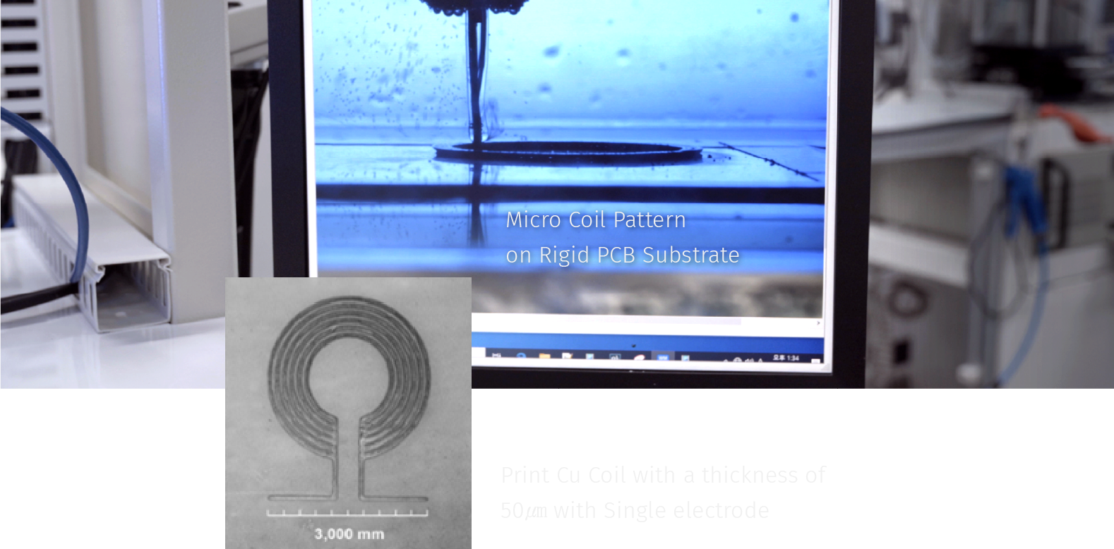
AMEBA 3D can print microelectronic components based on 3D CAD data, and the diameter of the electrode and 3D printing conditions should be optimized according to the required dimensional accuracy and surface roughness. To obtain the uniformity of metal structure inside the component, it is important to optimize the conditions such as the current/voltage and the gap between electrode and substrate using the software algorithm according to the geometry and position of electrode.
02
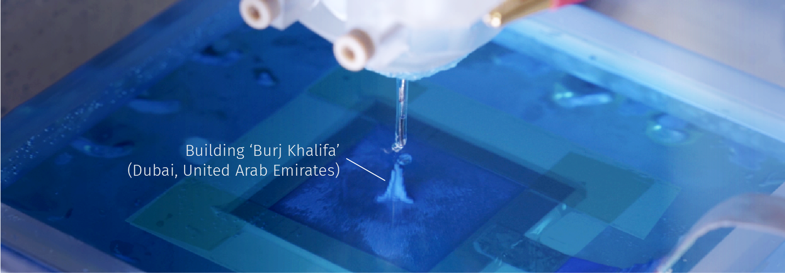
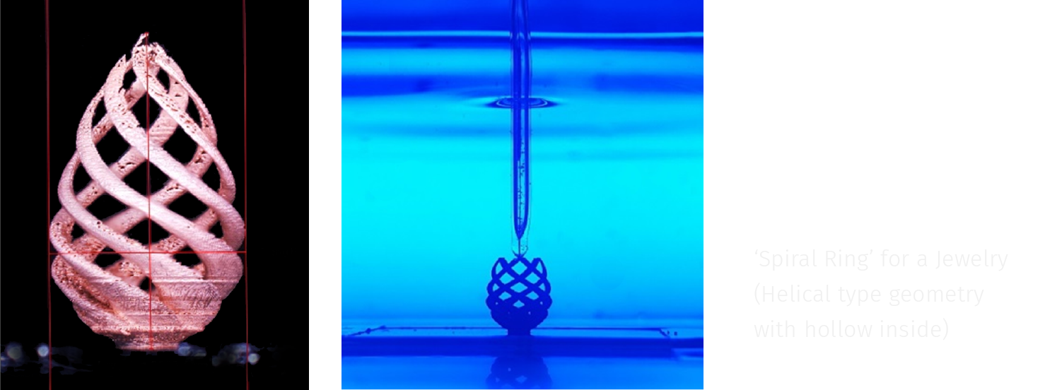
AMEBA 3D can analyze complex 3D CAD data and print fully 3D geometry of high complexity having empty spaces inside
it for the manufacturing of complicated Micro-Mechanical parts and Art products. The moving path of the electrode
and the gap between electrode and product should be optimized using the software algorithm developed for many
years through the analysis of 3D printing experimental data.
03
AMEBA 3D is printing high-temperature thermal resistant bonding material (Ag) on the ceramic substrate for high-power
semiconductors such as Active Metal Brazing (AMB) and Direct Bonded Copper (DBC). AMEBA 3D can directly print cir
cuits on the PCB substrate for high-power semiconductor using the optimized multi-electrode, through the DfAM (De
sign for Additive Manufacturing) which makes the design of high-power semiconductors suitable for 3D printing.