Making the Future
of
Electronic Components
for Semiconductor, Automotive,
Defense & Aerospace, and ICT & Healthcare
Industry
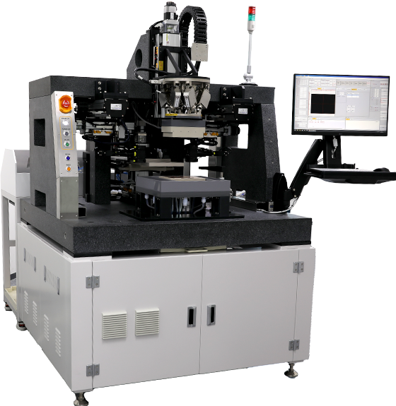
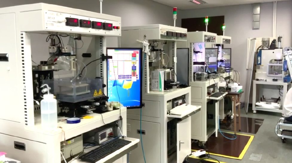
S-ECAM
Selective ElectroChemical Additive Manufacturing