AMEBA 3D
for 3D Circuit Printing
The superscript CR stands
for Circuit in AMEBA 3D CR
CR means Circuit
We want to give you the freedom
to 3D print high-resolution
or very thick electronic
circuits, bumps and bonding
layers through the AMEBA 3D
(S-ECAM for 3D Circuit) series
of machines.
01
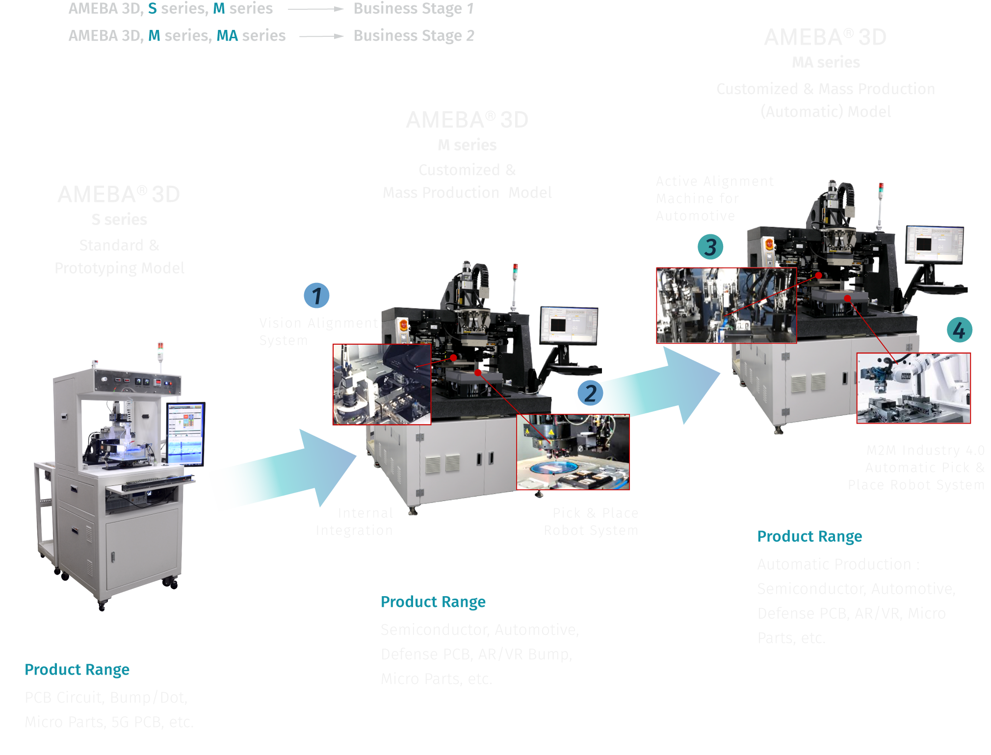
AMEBA 3D S series, as the Standard & Prototyping Model, is the equipment for prototype production and basic research in research institutes and production plants. AMEBA 3D M series, as the Customized & Mass Production Model, is the mass production equipment which is designed and customized for the production line of the mass production plants. AMEBA 3D MA series is the automated mass production equipment, and it is scheduled to be optimized and customized for the production line of the mass production plants by combining the automatic Active Alignment system and the M2M Industry 4.0 Automatic Robot system.
02
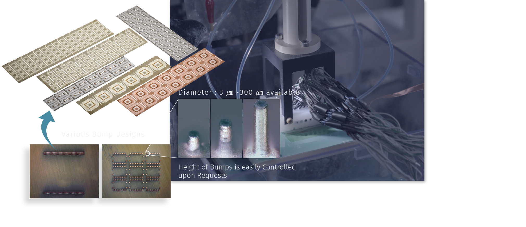
After manufacturing the multi-electrode module optimized for S-ECAM in strip size, AMEBA 3D mounts it, and prints
wafer bumps with high productivity and dimensional accuracy. AMEBA 3D can cover 3 ~ 300 ㎛ diameter and 10 ~ 500 ㎛
height of bumps within the aspect ratio of 1:5.
03
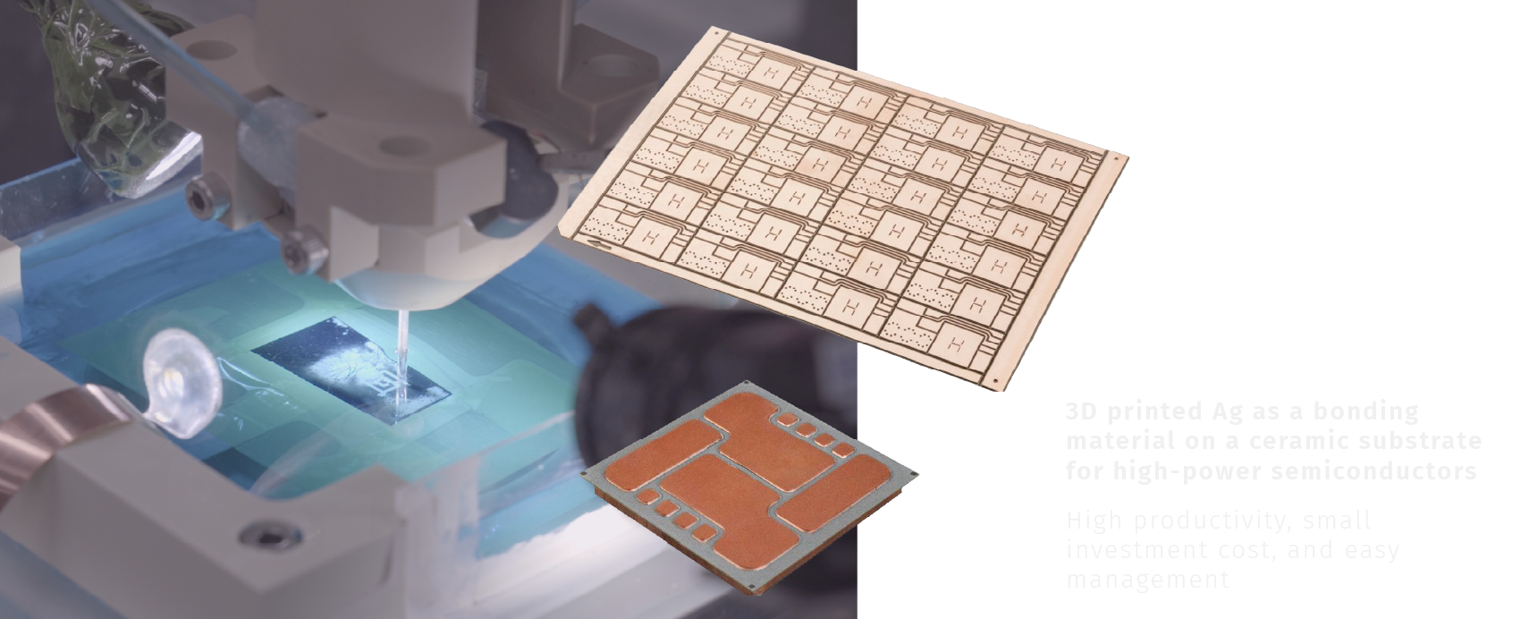
AMEBA 3D is printing high-temperature thermal resistant bonding material (Ag) on the ceramic substrate for high-power
semiconductors such as Active Metal Brazing (AMB) and Direct Bonded Copper (DBC). AMEBA 3D can directly print cir
cuits on the PCB substrate for high-power semiconductor using the optimized multi-electrode, though the DfAM (Design
for Additive Manufacturing) which makes the design of high-power semiconductors suitable for 3D printing.
04
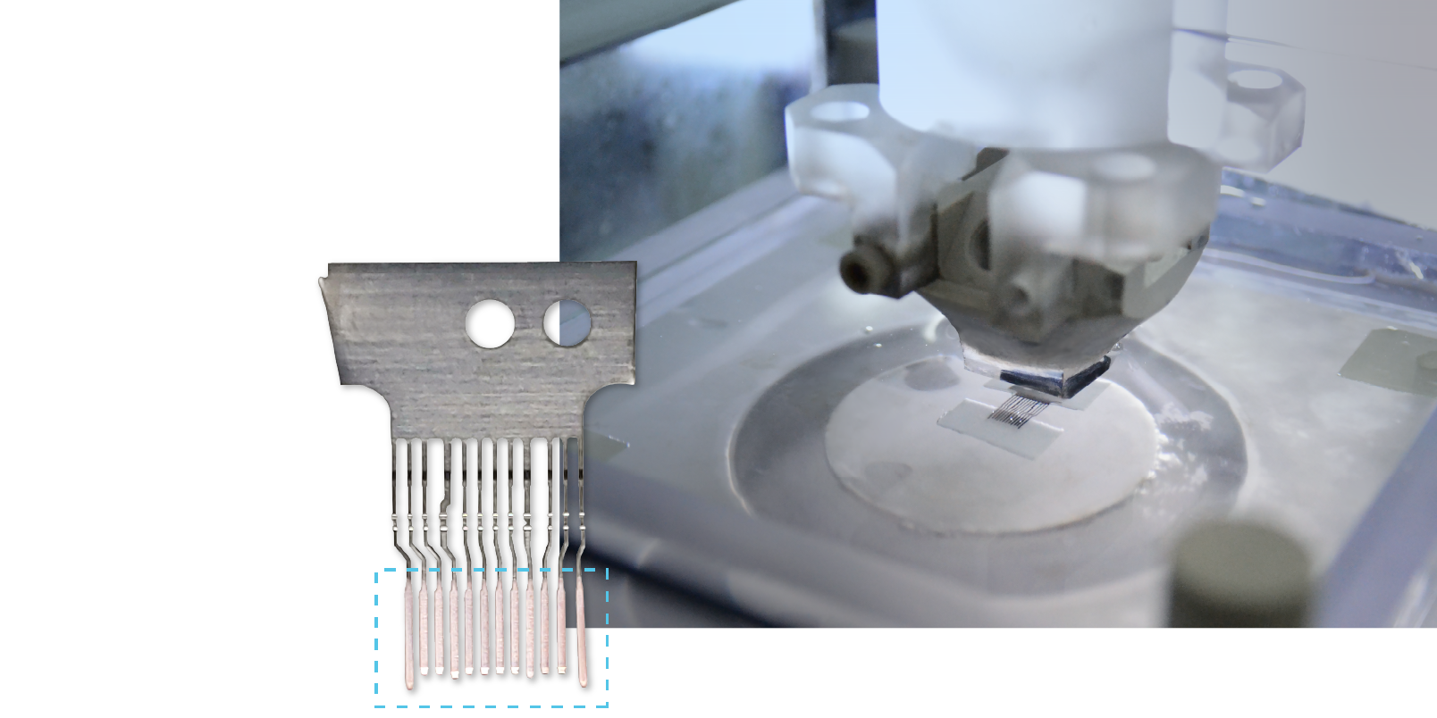
AMEBA 3D gives electrical conductivity functionality by 3D printing Ag or Au on a specific area of the structural material
made of thin plate stainless steel in the manufacture of the connectors for small electronic products with precise di
mensions. The electrically conductive layer uniformly plated through the printing by AMEBA 3D can bring about reduc
tion in electrical signal noise and stabilization of micro current fluctuation.