Selective Electrochemical
Additive Manufacturing
We want to give you the freedom
to 3D print high-resolution
or very thick electronic
circuits, bumps and bonding
layers through the AMEBA 3D
(S-ECAM for 3D Circuit) series
of machines.
01
S-ECAM stands for Selective Electrochemical Additive Manufacturing. S-ECAM can print circuit line width of 1 to 5,000 ㎛ and line thicknesses of 1 to 1,000 ㎛ and it is possible to print line with an aspect ratio of 1:5 or more and Line & Space of 20 ㎛ or less, respectively. Since S-ECAM prints in the state of metal ions, the electrical conductivity of the product is almost the same as that of pure metal (in the case of pure copper, 5.96 X 10⁷ S/m), and any metal that can be plated can be printed, such as Cu, Ni, Ag, Au, Pt, Sn, and so on.
02
When manufacturing wafer bumps with a thickness of 50 ~ 200 ㎛ for normal semiconductors, or patterns with a thick
ness of 10 ~ 5,000 ㎛ for high-power semiconductors, if the subtractive manufacturing is performed by the wet etching
method, the Total Processing Amount (TPA) is significantly increased, and complex and expensive masking process
should be involved. Conversely, if the additive manufacturing is performed using S-ECAM, the TPA is greatly reduced,
the masking process can be eliminated, and extremely small line & space can be obtained.
To manufacture wafer bump with the MSAP Modified Semi Additive Process, the 7 equipment and peripheral
devices such as Asher, Laminator, Lithographer, Developer, Stripper, Etching, Electroplating are required. It is estimated
that the cost for equipment investment is about USD 2.4 Mil. and the operating cost is about 0.2 Mil. In comparison, the
use of S-ECAM can reduce the cost of equipment and peripherals to about USD 1.1 Mil and operating cost to about USD
0.03 Mil, and the sum of these two costs is less than half that of MSAP.
03
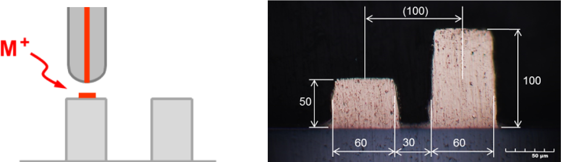
In the conventional PCB process, pattern formation is fabricated through selective plating or etching using dry film.
However, it is impossible to produce a pattern with a high aspect ratio due to the dry film resolution and the difficulty
of the etching process. S-ECAM technology can selectively produce high aspect ratio patterns effectively, and the Line
and Spacing can be controlled with the diameter of electrode for printing.
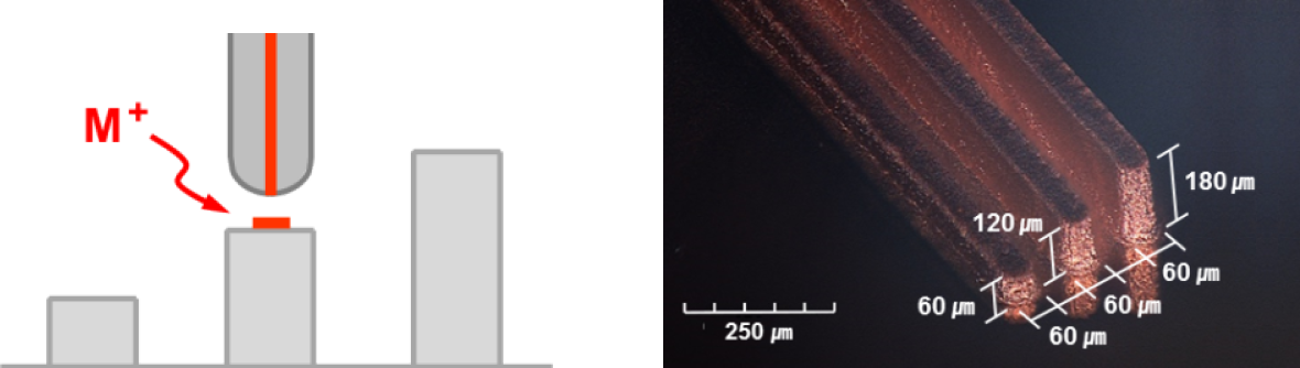
Have you ever felt the temptation to print a circuit of various thicknesses on a PCB board? S-ECAM can manufacture the
various thickness and shape of the patterns on a PCB substrate. So, it allows increased Design of Freedom and reduced
PCB size. The Line & Spacing can be controlled with the diameter of electrode for printing.
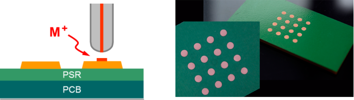
S-ECAM can printing an electric circuit or pattern on the surface of the PCB substrate coated with an insulating material such as substrate can help improve the performance of 5G or other antennas.