Challenge for
Line Width of Wafer Bumps
When EUV equipment implements
the semiconductor line width in
Ångström units, we want to enable
you to implement the required line
width in nano units on the PCB.
01
In 1892~1895, Albert A. Michelson defined the ångström so that the red line of cadmium was equal to 6438.47 ångströms. In 1907, the International Union for Cooperation in Solar Research (which later became the International Astronomical Union) defined the international ångström by declaring the wavelength of the red line of cadmium (in dry air at 15 °C (hydrogen scale) and 760 mmHg under a gravity of 9.8067 m/s2) equal to 6438.4696 international ångströms, and this definition was endorsed by the International Bureau of Weights and Measures in 1927. (Wikipedia)

02
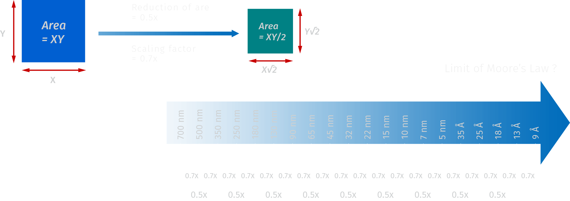
In Semiconductor Packaging, S-ECAM technology will be able to make it possible to print Nano-sized line widths
on PCBs to correspond to Ångström(å)-sized line width of Semiconductors.

The density of Integrated Circuits (IC) is double, every time the line width of a Semiconductor is reduced by a
factor of x0.7. Will this rule continue even when the line width is reduced to Ångström units of less than 1 nm ?