Wafer Bumping for
Line Width made by EUV
When EUV equipment implements
the semiconductor line width in
Ångström units, we want to enable
you to implement the required line
width in nano units on the PCB.
01
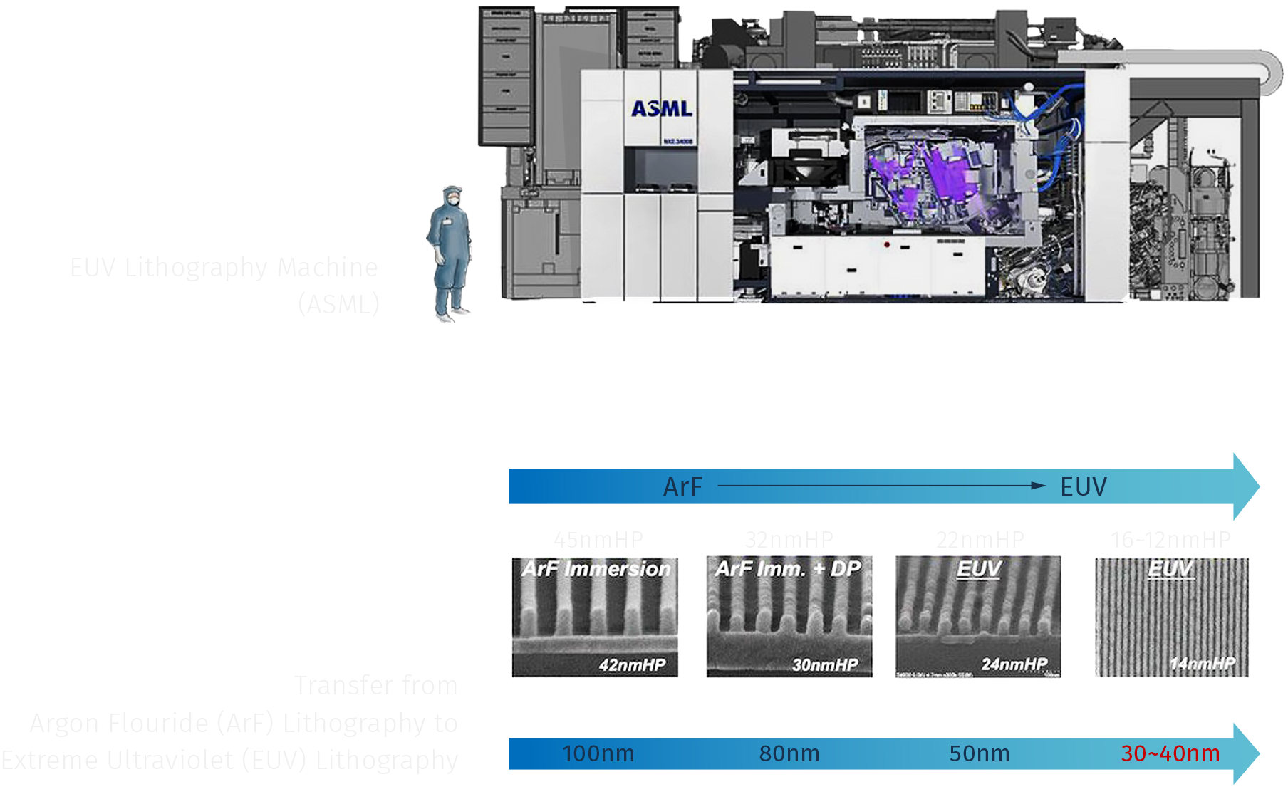
EUV (Extreme Ultraviolet) method makes the micro processing up to 14 nm possible only with single patterning, and if multi-patterning technology is also introduced into EUV, it is theoretically possible to process up to 2 nm or less. EUV single patterning can reduce costs by 15~50% compared to the existing DUV (Deep Ultraviolet) multi-patterning method using ArF (Argon Fluoride Immersion), reduce cycle time by 3-6 times, and improve performance due to low heat and low power.
02
If the EUV technology reduces the line width of the Semiconductor to 2~5 nm or less, the Diameter of the Bump on
the PCB connected to it should also be reduced to 5~20 ㎛ or less at the same time.
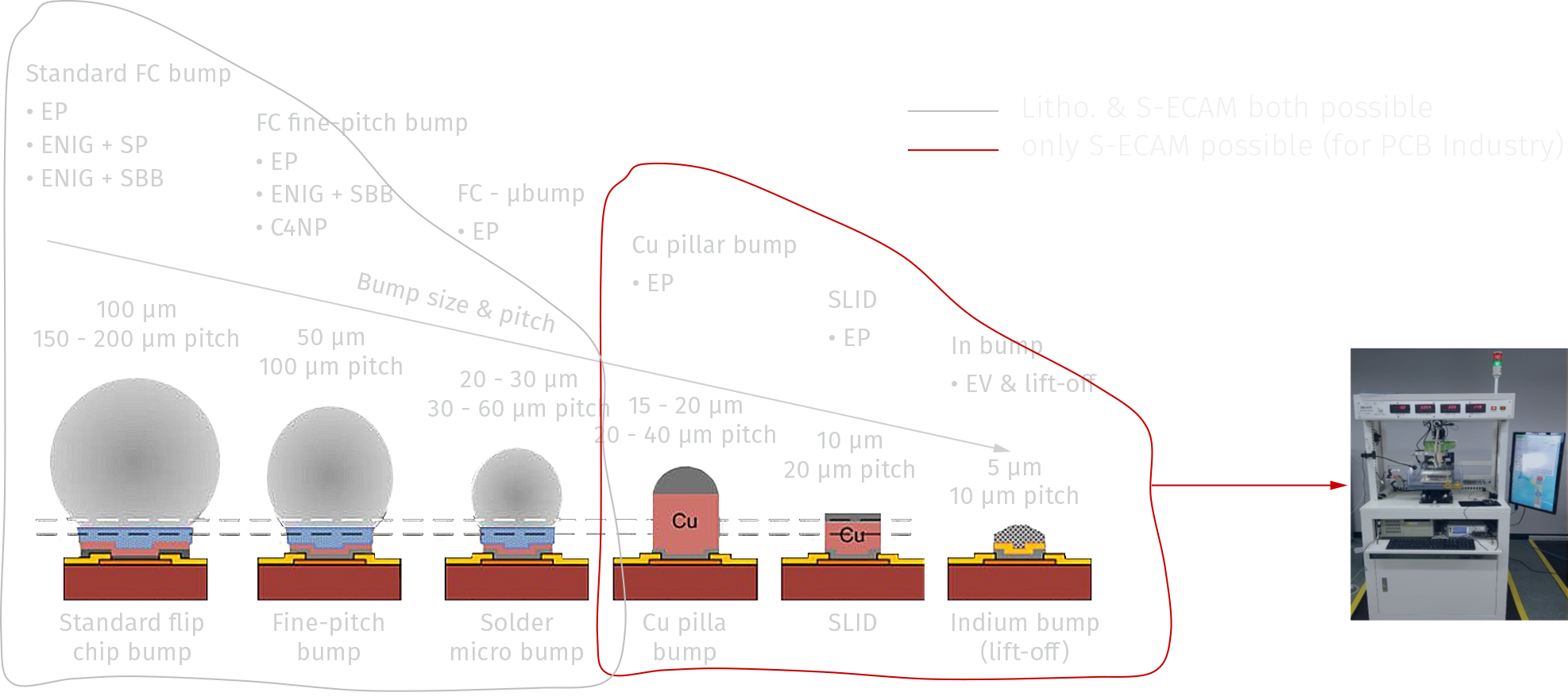
S-ECAM can accurately print Bumps with the diameter of 5~20 ㎛ or less on the PCB, and it is also possible to ad
dress the exact location. This is possible because the Bump is directly printed with the Electrode of the same di
ameter in S-ECAM technology.